Boron and Phosphorus Diffusion in SiO2 and SiOxNy
Summary
Extensive data exists on boron penetration in thin thermal oxides, because of the importance of this effect in CMOS manufacturing. Much less work has been done on phosphorus, whose solid state diffusivity is much less than that of B.
For both boron and phosphorus, high concentrations and high temperatures lead to the formation of a liquid or quasi-liquid melt phase in which transport is rapid. The concentrations required (at least for B) are well-described by the bulk phase diagram for temperatures > 1000°C. An underlying thermal oxide is dissolved readily until the concentration in the melt falls below the liquidus.
Solid-state diffusion in SiO2 is much slower than transport in the "melted" phase. Diffusion of P is much slower than that of B. The diffusion of B is also strongly influenced by the ambient: H2 and F can cause 10-40X increases in diffusivity vs. N2 ambients. Small additions of nitrogen in the oxide strongly inhibit boron diffusion.
Very little has been published on the diffusivity on either dopant in CVD films as opposed to thermal oxides. The work I have found dates from the early 70's, and characterization of the deposited glasses involved is rather primitive. However, it seems clear that diffusion of boron (at least) in some CVD films is up to 100X faster than in thermal oxide. It is not clear what role is played by e.g. H impurities in the deposited films, vs. defects and porosity.
Activation energies are typically 3.5 eV for solid-state diffusion of B in SiO2; those reported for P in SiO2 vary widely. Typical values (cm2/s) at 1100°C are
ambient
medium
D[P]
D[B]
H2 SiO2 1.5x10⁻¹⁷ 1x10-15 N2 SiO2 3x10-18 3x10-17
Literature Review
General Remarks
The majority of the literature I have unearthed on these subjects dates from 1975 or earlier; the only issue investigated in detail since then is the diffusion of boron in thin gate oxides, which is critical to fabrication of p-MOS FETs using boron-doped polysilicon as a gate material. Much of this work is primarily concerned with control of silicon surface concentrations during intentional diffusion doping; in many cases, the sources of dopants are not e.g. doped oxides deposited by CVD, but doped glasses formed during high-temperature diffusions from e.g. POCl3 or B2O3 sources in oxidizing atmospheres.
High Temperature Diffusion: Glass Formation
Diffusion of boron and phosphorus into pure silicon dioxide requires that a region of high concentration of B or P act as a source for the diffusion. The addition of boron or phosphorus to silicon dioxide causes large reductions in the glass transition temperature and melting temperature. If the diffusion temperature exceeds the melting temperature for these high-concentration regions, they will liquify. Further, neighboring undoped oxide will dissolve rapidly until the consequent dilution of the liquid region reduces the concentration of boron or phosphorus and the molten region begins to solidify. This dissolution proceeds much more rapidly than solid-phase diffusion of trace boron or phosphorus through thick oxides, and thus is the primary means of transport when it occurs. The process is depicted schematically for boron in figure 1, after Brown and Kennicott [1].
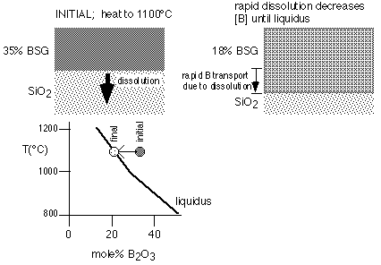
Figure 1: Melting of Doped Oxide and Dissolution of SiO2 , with consequent transport of dopant
The kinetics of dissolution and transport in the liquid/solid mixture can be quantified as was done by Ghoshtaghore [2], but it seems likely that for most purposes the formation of the melt and dissolution of neighboring oxide can be treated as instantaneous relative to solid state diffusion; thus, transport due to this mechanism can be treated based on the phase diagram for the dopants in question [3].
Solid-State Diffusion of P in SiO2
True solid-state diffusion of phosphorus through silicon dioxide is quite slow and often negligible; most of the data dates from 1975 or earlier and focuses on high-temperature processes (>1100°C).
In table I we summarize solid-state diffusion coefficients for phosphorus in SiO2 using various diffusion ambients. Data is extrapolated to 1100°C. Activation energies are frequently based on a temperature range too small to consider them very reliable. SiO2 is thermally grown from the single-crystal substrate unless otherwise stated.
Table 1: Summary of Phosphorus Diffusion in SiO2
ambient
medium
D[P] cm2/s
Ea (eV)
reference H2 SiO2 1.5x10⁻¹⁷ 4.0 [4] N2 SiO2 3x10-18 4.4 [4] Ar PSG* 3.5x10⁻¹⁶ 4.4 [2]
* This quantity actually appears to be the diffusion coefficient associated with the loss of phosphorus to the ambient due to evaporation during the diffusion; it is thus a diffusivity through a doped glass surface. The author remarks that it is independent of phosphorus concentration.
The observed diffusion coefficients are very small: for example, the diffusion length in pure SiO2, even in a hydrogen ambient, is only about 1.2 nm for a 1 hour diffusion at 1000oC.
Solid-State Diffusion of B in SiO2
The diffusion of boron is much faster than that of phosphorus, and in consequence represents a signficant technological problem for p-MOSFETs in which the p-doped polysilicon represents a source of B which can diffuse through the gate oxide. Thus active research on boron diffusion in oxides has continued up to the present.
In table II we summarize data on diffusion in various ambients and films deposited by differing techniques, selecting the data at either 800 or 1100°C for simplicity. Most of this data is shown graphically in figure 2. The lines in the figure have a slope corresponding to an activation energy of 3.5 eV, approximately equal to the average of the activation energies listed in table II.
Table 2: Summary of Boron Diffusion in SiO2
ambient
medium
T (oC)
D[B] cm2/s
Ea (eV)
reference Ar SiO2 1100 6x10-17 4.06 [5] Ar SiO2 1100 5x10-17 3.9 [1] N2 SiO2 1100 2x10-16 -- [4] O2 SiO2 1100 2.2x10⁻¹⁶ -- [4] steam SiO2 1100 4x10-16 -- [4] H2 SiO2 1100 2.8x10⁻¹⁵ -- [4] N2 SiO2* 1100 3x10-17 3.5 [7] H2 SiO2* 1100 1x10-15 3.0 [7] N2 SiO2 1100 7x10-17 3.5 [8] H2 SiO2 1100 1x10-15 3.6 [8] N2 SiO2* 1100 2.5x10⁻¹⁷ 2.3 [8] H2 SiO2* 1100 3x10-15 3.0 [8] ? PETEOS SiO2, 300 mT 1100 8x10-15 2.6 [6] ? PETEOS SiO2, 150 mT 1100 2x10-14 2.6 [6] N2? SiO2 800 3.5x10⁻²⁰ 3.8 [9] N2? SiO2 [1016/cm2 F coimplant] 800 1x10-18 3.6 [9] N2? SiO1.8N0.2 800 9x10-21 4.4 [9] N2? SiO1.8N0.2 [1016/cm2 F coimplant]
800 5x10-19 3.8 [9]
* These values use B implanted directly into SiO2 as a diffusion source.
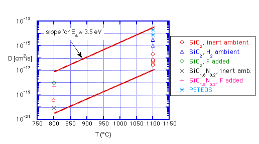
Figure 2: B diffusion in SiO2 and SiON, various conditions, data from table II; reference lines depict activation energy of 3.5 eV
We can draw the following conclusions:
- Data for diffusion rates in pure thermal oxide in inert ambients are consistent between different reports;
- Implantation of boron directly into the oxide leads to a reduced diffusion rate;
- Diffusion in H2 leads to a marked increase in diffusion rate, with very consistent results by several workers;
- F added (typically by co-implant or from BF2) has an effect similar to that of H2 ambient
- Modest additions of nitrogen reduce the diffusion rate significantly
- Diffusion in CVD oxides is faster than in thermal oxide (one report)
Qualitative support for some of these conclusions comes from other work as well. Morimoto et. al. [10] and Uchiyama et. al. [11] both studied diffusion of B from poly through thin thermal oxides, and found that modest additions of nitrogen eliminated MOSFET degradation due to boron penetration even for 2 nm oxides. They note that thinner oxides show higher diffusion rates, and suggest that F from the poly doping implants is the cause.
Hydrogen and fluorine both act to reduce network connectivity: H can stabilize non-bridging oxygen atoms by forming Si-OH, or attach directly as Si-H (less favorable). F forms a very strong bond with Si and the resulting Si-F is probably non-bridging. In either case, the total number of bonds holding a silicon atom in place are reduced. Since both these additions have large effects on the diffusivity of B, we can guess that boron diffuses substitutionally by some defect-migration mechanism; the migration of the defects would be aided by Si atoms of reduced coordination (more weakly bound).
Nitrogen, on the other hand, increases the coordination and density of the lattice, since it is trivalent (bonds to 3 silicons, vs. 2 for oxygen). The strong effect of small concentrations of nitrogen suggests that the nitrogen sites act to pin defects and prevent their migration.
Fast migration through CVD oxides may be related both to reduced density and to the presence of such impurities as hydrogen or carbon; in the absence of detailed characterization of the CVD oxide we cannot disentangle these effects.
Boron is a trivalent atom, and is probably incorporated into the oxide lattice in a planar configuration bonded to three oxygen atoms. As a neutral atom is it very small; Harrison [12] gives the covalent diameter as 1.5 Å. Phosphorus, on the other hand, has multiple valence states and is believed to incorporate into the oxide lattice in a tetrahedral coordination state bonded to four oxygen atoms, just as silicon does. It is also larger, about 2.35 Å in diameter. There are thus several plausible reasons why boron would diffuse faster than phosphorus: it has fewer bonds to break in order to move from place to place, and as an interstitial it is smaller and can fit through voids or pores more easily.
Fair [14] proposes that diffusion of boron and phosphorus in silicon dioxide proceeds via peroxide defects, that is:
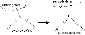
Fig. 3: Proposed model for boron diffusion in silicon dioxide, after [14]
Fair proposes that since the diffusion is via breaking and making bonds to the neighboring O atoms, the activation energy for diffusion should scale with the heat of formation of the relevant oxide (of B or P). He then shows reasonable agreement between diffusion activation energies and heats of formation for the relevant oxides (which hardly seems a compelling argument for this specific mechanism!). He also proposes explanations for the effects of F, H, and N: in particular, he claims that nitrogen atoms will insert into the peroxide defect to form Si-O-N-O-Si. While I'm skeptical of many of the assertions in this paper, it at least provides a starting point in thinking about the mechanisms. If he's right, then Si-rich oxides should be good diffusion barriers due to a paucity of O and therefore peroxide, but oxidation of such oxides should produce porous oxides as O2 insertion into Si-Si links occurs.
Hasegawa et. al. [15] studied various ways of preparing nitrided oxides. They found that the presence of N at both the Si-oxide interface and the surface, obtained by oxidation in N2O, was best for preventing boron diffusion. This enabled them to employ very thin insulating films ( 50-60 Å) without degradation in transistor threshold voltage, charge to breakdown, or electron trap generation properties. It is interesting to note that they imply that the diffusion of B into the oxide is by itself a cause of breakdown degradation, and that part of the action of nitrogen in improving charge-to-breakdown Qbd is simply to prevent this in-diffusion.
Multilayer CVD Oxides: Some Thoughts
What concern must we have for dopants diffusing from a CVD oxide (e.g. the first interlayer dielectric, often BPSG) to the substrate?
From figure 2 we can see that diffusion of boron in oxides is very slow for temperatures less than 1000°C: for example, at 950°C a reasonable upper bound on diffusivity would be about 5x10-16 cm2/s, even allowing for initially porous oxides with hydrogen present. For a 20 minute exposure this corresponds to a diffusion length of about 150 Å; a 500 Å undoped barrier would be quite adequate to avoid penetration through the film. Phosphorus will move more slowly. Thus we can probably ignore solid state diffusion in most cases.
Combined dissolution/diffusion is somewhat more subtle. If an overlayer of BPSG is being used as a flow glass, it will by definition be raised to temperatures near the glass transition (i.e. the viscosity of the glass will be reduced). I have discovered no publications on the behavior of an underlying layer during flow, but at least one report describes use of an undoped cap on a BPSG layer [13]. The undoped cap layer was chosen to be 100-200 Å thick; Auger analysis showed modest dopant penetration into this cap at 850°C for 45 minutes. Note that from figure 2, a reasonable guess for diffusivity of boron at this temperature might be 10-18 to 10-17 cm2/s, resulting in a diffusion depth of 10-30 Å. Anecdotal evidence of similar behavior was obtained in CVD work by the present author: in deposition of a CVD doped oxide in a single-wafer reactor, dopant flows were turned off before SiH4, leading to a thin undoped layer on the surface, probably 200 Å thick. This layer retained its configuration upon heating to 900°C on the tops of steps, but flowed readily in trenches, where due to poor step coverage the thickness was probably reduced by a factor of 2-3. Thus we can guess that during typical flow processes dopants will penetrate <100 Å into an undoped SiO2 film. This result is consistent with the assumption that typical flow temperatures do not liquify the glass sufficiently for dissolution to play a role, since ample dopants are available to completely convert the cap layer without significant dilution of the "melt".
Metrology
The method of choice for most purposes is clearly SIMS profiling. For thick oxides the profiles of boron and phosphorus can be measured directly; for penetration through thin oxides or where diffusion in the oxide is a small effect, one can measure the diffusion into underlying silicon. Penetration through thin oxides can also be studied by examining changes in flatband voltage of MOS capacitors formed on the oxide or in MOS transistors, although such methods are more appropriate in a fab environment than an equipment manufacturer.
Much of the older work on this subject was oriented towards controlled diffusions into silicon, and thus employs the resulting profiles in an underlying silicon substrate to measure diffusion through an oxide film. In the 60's and 70's the resulting doped profiles were evaluated by removing the oxide layers and measuring the sheet resistance (4-point probe) and junction depth (lap and stain). Such an approach can certainly be used for "quick and dirty" experiments today: changes in sheet resistance are very easy to monitor and can be used as a quick check for penetration through a barrier.
Some workers also employed neutron activation analysis combined with oxide stripping to directly measure profiles of phosphorus. This technique is in principle quantitative but laborious and expensive.
References
1 "Glass Source B diffusion in Si and SiO2", D. Brown and P. Kennicott, J. Electrochem. Soc. 118 293 (1971)
2 "Silicon Dioxide Masking of Phosphorus Diffusion in Silicon",R. Ghoshtagore [Westinghouse], Solid State Electronics 18 399 (1975) and "Phosphorus Diffusion Processes inSiO2 Films" same author, Thin Solid Films 25 501 (1975)
3 "Silica-Based Oxide Systems" (parts I and II), G. Baret, R. Madar, and C. Bernard, J. Electrochem. Soc. 138 2830 (1991)
4 "Boron and Phosphorus Diffusion through an SiO2 layer from a Doped Polycrystalline Si Source under Various Drive-in Ambients", K. Shimakura, T. Suzuki, and Y. Yadoiwa [NEC], Solid State Electronics 18 991 (1975)
5 "The Diffusion of Boron in the Si-SiO2 System", P. Wilson, Solid State Electronics 15 961 (1972)
6 "Studies on diffusion of Boron through Silicon Oxide Films", S. Mukherjee and P. Evans [U Manchester], Thin Solid Films 14 299 (1972)
7 "The Effect of Hydrogen on Boron Diffusion in SiO2", Y. Shacham-diamand and W. Oldham [UC Berkeley], J. Elect. Mater. 15 229 (1986)
8 "Ambient and dopant effects on boron diffusion in oxides", C. Wong and F. Lai [IBM], Appl Phys Lett 48 1658 (1986)
9 "Effect of fluorine on boron diffusion in thin silicon dioxides and oxynitride", T. Aoyama, K. Suzuki, H. Tashiro, Y. Toda, T. Yamazaki, K. Takasaki, and T. Ito [Fujitsu], J. Appl. Phys. 77 417 (1995)
10 "Effects of boron penetration and resultant limitations in ultra thin pure-oxide and nitride-oxide gate films", T. Morimoto, H. Momose, Y. Ozawa, K. Yamabe and H. Iwai [Toshiba], Technical Digest, International Electron Devices Meeting 1990 p. 429
11 "High Performance Dual-gate Sub-halfmicron CMOSFETs with 6 nm-thick Nitrided SiO2 Films in an N2O Ambient", A. Uchiyama, H. Fukuda, T. Hayashi, T. Iwabuchi and S. Ohno [Oki], Technical Digest, International Electron Devices Meeting 1990 p. 425
12 Electronic Structure and the Properties of Solids, Walter A. Harrison, W. H. Freeman, 1980 [ISBN 0-7167-1000-5], solid state table
13 "Suppression of Water Absorption in (BPSG) Thin Layers with High Boron Concentration", K. Nauka and C. Liu (HP), J. Electrochem. Soc. 138 2367 (1991)
14 "Unified Model of Boron Diffusion in Thin Gate Oxides: Effects of F, H2, N, Oxide Thickness and Injected Si Interstitials", R. Fair, Technical Digest, International Electron Devices Meeting, 1995, p. 85
15 "The impact of nitrogen profile engineering on ultra-thin nitrided oxide films for dual-gate CMOS ULSI", E. Hasegawa, M. Kawata, K. Ando, M. Makabe, M. Kitakata, A. Ishitani, L. Manchanda, M. Green, K. Krisch and L. Feldman, Technical Digest, International Electron Devices Meeting, 1995
Selected Shorts Table of Contents
| ambient | medium | D[P] | D[B] |
|---|---|---|---|
| | | | |
| | | | |
| ambient | medium | D[P] cm2/s | Ea (eV) | |
|---|---|---|---|---|
| | | | | |
| | | | | |
| | | | | |
| ambient | medium | T (oC) | D[B] cm2/s | Ea (eV) | |
|---|---|---|---|---|---|
| | | | | | |
| | | | | | |
| | | | | | |
| | | | | | |
| | | | | | |
| | | | | | |
| | | | | | |
| | | | | | |
| | | | | | |
| | | | | | |
| | | | | | |
| | | | | | |
| | | | | | |
| | | | | | |
| | | | | | |
| | | | | | |
| | | | | | |
| | [1016/cm2 F coimplant] | | | | |