High-Density Plasma CVD of SiO2
None of the approaches we've so far examined for depositing silicon dioxide can simultaneously achieve good conformality and high film density at low deposition temperatures (<400 °C). During the early 90's a film that met all those requirements became increasingly necessary for intermetal dielectric applications in etched-aluminum processing. Processes graduated to 4-6 layers of metal, butto maintain electromigration lifetime, metal thickness wasn't scaled down as fast as the lateral dimensions were shrinking; as a consequence, the aspect ratio of the gaps between metal lines increased. Smaller features meant stricter requirements on aluminum surface topography to avoid etching problems; high temperatures (above 400 °C) caused hillocks to grow in the aluminum. Finally, smaller transistors with thin oxides were vulnerable to reliability degradation due to migration of water incorporated in dielectric materials such as TEOS-ozone-based SiO2 or spin-on glasses.
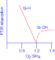
In the mid-80's, workers in Japan and elsewhere had shown that the hydrogen incorporated in conventional plasma oxides can be removed, even at very modest deposition temperatures, if enough ion bombardment can be provided; the example data shown below is due to Karen Seaward when she was at Hewlett-Packard:
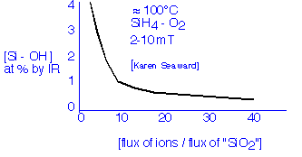
For reasonably high deposition rates, we need a very high plasma density to achieve significant ion bombardment effects. Let's define for convenience High Density Plasma Deposition as occurring when the ion flux to the surface is larger than the net deposition flux. (In this case, every deposited atom gets whacked by an ion at least once on the average.) The ion flux is estimated from the Bohm velocity and the plasma density. The deposition flux can be calculated from the deposition rate and the molecular density. Let's take an example: for deposition of silicon dioxide at 1000 Å/minute, the molecular flux to the surface is 3.8x10¹⁵ molecules/cm2 second; this is equivalent to an electric current (of singly charged ions) of about 0.6 mA/cm2. By reference to our previous calculations we find that the plasma density required at the sheath edge to produce such a flux is at least 1010 ions/cm3.
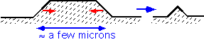
If we can combine such high densities with a reasonably low pressure and some bias voltage on the sheath, we can get an additional benefit: significant sputtering of the deposited film. This backhanded method of deposition (put it on and then take it off??) can be useful because the sputtering rate is dependent on the angle. However, there's a tradeoff: the higher the aspect ratio of the gap you're trying to fill, the more sputtering you need and thus the lower the net deposition rate (and wafer throughput) are.
Let us define an angle of incidence for incoming species:
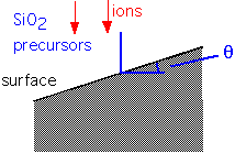
As the angle varies (which happens when the film is deposited over features such as trenches or holes), the deposition rate and the sputtering (etch) rate vary:
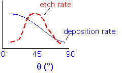
The film will grow most rapidly on the surfaces which are nearly horizontal, with surfaces inclined around 45-50 degrees growing slowly due to the high sputter etch rate. As the surface propagates upward the slowest-growing planes will dominate the curved parts of the surface...
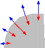
...forming "facets" inclined to the surface, which eventually meet and partially annihilate. The net result is that holes and trenches will tend to be filled up and planarized (if their initial aspect ratio isn't too high!).
More details on how this works can be found in "Profile Simulation of Plasma Enhanced and ECR Oxide Deposition with Sputtering"; C. Chang, J. McVittie, K. Saraswat, S. Lassig, J. Dong; 1993 Int'l Electron Devices Meeting, Washington DC, technical digest p. 853.
So if we combine high plasma density and low pressure, we can get some neat benefits: high film quality at low deposition temperatures, and nice gap-filling and planarization properties at the same time. However, conventional showerhead reactors cannot achieve the high plasma densities cited above at low operating pressures. New reactor designs and operating principles are needed (and as we'll see, new problems arise).
HDP films deposited at less than 300 °C are essentially as dense as thermal oxides, and do not shrink upon anneal even to 900 °C, unlike all other low-temperature deposited films. Along with densification comes compressive stress. Since HDP films are dense and compressive, cracking on anneal is not an issue. However, excessive compressive stress can lead to metallization reliability problems. By applying high RF bias power (typically 500-1000 W on a 200 mm wafer), high sputtering rates can also be achieved, giving excellent step coverage and gap fill ability. See our discussion of HDP reactors for details on consequent reactor design issues.
Process Chemistry
Silane, SiH4, is almost universally employed as the precursor for HDP deposition; TEOS has been tried but confers no significant advantages. A mixture of oxygen and argon is added to provide the oxidant and the sputtering agent. The very high density of energetic electrons in the reactor means that the silane is readily cracked at low temperatures, so that in the absence of oxygen, amorphous silicon films will result. Thus, any stoichiometry from hydrogenated silicon to pure silicon dioxide can be deposited. This flexibility is also a process challenge: good control of the gas mixtures is required to deposit pure, hydrogen-free silicon dioxide. Excessive silane leads to Si-H in the films, whereas too much oxygen gives Si-OH groups.
[Lassig, AVS HDP Source Workshop, San Francisco, 1993]
Intentional operation in the silicon-rich regime provides films with good moisture-gettering properties, since the Si-H bonds will react with water molecules to form Si-OH and molecular hydrogen.
Increase of ion bombardment flux, ion energy, or increase of substrate temperature reduce the amount of hydrogen incorporated in the films. It is possible to deposit very low hydrogen films at near room temperature, but at the cost of reducing deposition rate (to increase the ion flux: deposition flux ratio). The hydrogen removal appears to be more subtle than simple sputtering of hydrogen from the surface: increased ion bombardment is much less effective in removing hydrogen from silicon nitride, and kinematics shows that energy transfer from heavy ions such as argon or oxygen to hydrogen atoms is inefficient.
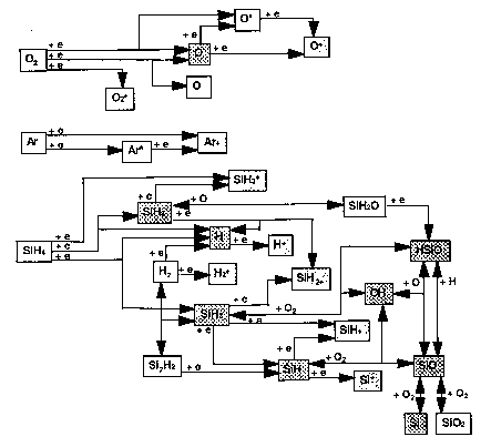
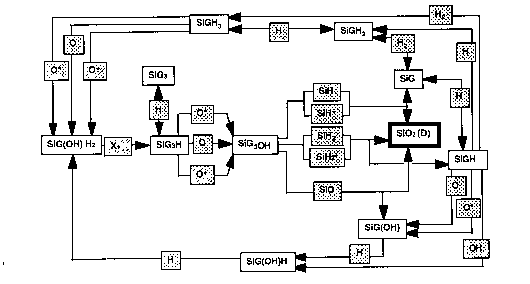
The chemistry of deposition is complex. Ellen Meeks and coworkers at Sandia Laboratories have constructed a partial model, including important gas phase and surface reactions but not stoichiometry (SiO2 is the only allowed solid). The results for dominant gas phase and surface paths are shown below.
Gas-Phase Reactions
Surface Reactions:
Conclusions
Oxide from high density plasmas, using RF bias on the substrate to enhance ion bombardment energies, has become an accepted approach to oxide deposition for low-temperature requirements. Originally developed for intermetal dielectrics, HDP oxides are also employed in isolation trench fill and dielectrics over polysilicon, as pre-metal thermal budgets have become more and more constrained. HDP is unique amongst methods of depositing silicon dioxide in its ability to produce dense films at low temperatures.
Additional references:
"Modeling High-Density-Plasma Deposition of SiO2 in SiH4/O2/Ar", E. Meeks, R. Larson, P. Ho, S. Han, E. Edelberg, E. Aydil and C. Apblett, Sandia Report SAND97-8241-UC 401 March 1997
"High Quality High Rate SiO2 and SiN Room Temperature Formation by Utilizing High Excited Ions" T. Fukuda, K. Saito, M. Ohue, K. Shima, and N. Momma, IEDM 1992 p.285
"Role of ions in electron cyclotron resonance plasma-enhanced chemical vapor deposition of silicon dioxide" K. Seaward, J. Turner, K. Nauka, and A. Nel, J. Vac. Sci. Technol. B13 118 (1995)
"Implementation of Electron Cyclotron Resonance Plasma SiO2 into Sub-half Micron Technology" C. Wang, Y. Huang, D. Pirkle, L. Liu, J. Wang, H. Cheng and M. Lin, DUMIC 1995 p. 29
"Low Temperature Chemical Vapor Deposition of High Quality SiO2 Film Using Helicon Plasma Source" Y. Nishimoto, N. Tokumasu and K. Maeda [SPL] Jpn. J. Appl. Phys. 34 1021 (1995)
"Study of surface reactions during plasma enhanced chemical vapor deposition of SiO2 from SiH4, O2 and Ar plasma" S. Han and E. Aydil, J. Vac. Sci. Technol. A14 2062 (1996)
"Ion Bombardment Induced Compositional Change in ECR-CVD SiO2 and SiN:H", D. Dobkin, K. Seaward, F. Mertz and K. Nauka, Proc. 13th Int'l Conf on CVD (Electrochemical Society Proc vol 96-5) p. 523 (1996)
"Characterization of High Density Plasma CVD USG Film", W. Lu, J. Zheng, J. Sudijuno, H. Yap, K. Fam, C. Leong, M. Liao, Y. Lin, in "Multilevel Interconnect Technology", ed. D. Patel and M. Graef, Austin, TX, October 1-2, 1997, SPIE vol. 3214 p. 94
Return to Tutorial Table of Contents
Book version of the CVD Tutorial