High-Dielectric-Constant Materials: Tantalum Oxide
Well, the applications material here is also pretty dated... but the film still seems worth a note, so here goes (March 2016).
Instant Review: DRAM Storage Capacitors
The single-transistor cell dynamic random access memory (DRAM) is the basic architecture for most commodity semiconductor memory chips; billions of chips are manufactured every year. A single cell, storing a bit of information, consists of a transistor and a storage capacitor. Placing a voltage on the word line to turn the transistor on allows the charge in the storage capacitor to be transferred to the bit line and read as a 1 or 0.
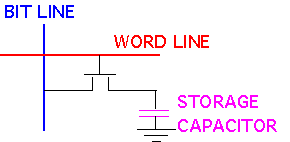
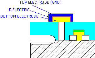
The storage capacitor is implemented in various configurations. One method, shown below, is to use form a cylindrical post above the transistors, deposit a dielectric layer on the post, and then deposit a top electrode.
The capacitance of the storage capacitor determines how much charge can be stored with the available voltage, and thus is crucial to successful miniaturization of the cell. The capacitance depends on the area, dielectric constant, and dielectric thickness:
In order to increase the capacitance, one can therefore follow three strategies:
- increase area: since the actual wafer area used by the capacitor can't expand or the chip size will grow, increasing capacitor area means using complex structures to increase the surface area available in a fixed projected area.
- decrease thickness: the minimum thickness of dielectric is typically limited by leakage currents; about one microamp/cm2 leakage is permissible at the applied voltage, which is 1/2 of the supply voltage. Current oxide-nitride-oxide sandwiches ("ONO" dielectrics) achieve a thickness of about 3.5 nm.
- increase dielectric constant: there's a lot of room in this direction, but it involves developing and integrating new materials into a semiconductor process. Some of the choices:
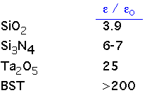
[BST is barium strontium titanate, a paraelectric material closely related to ferroelectrics.]
Tantalum oxide is a possible intermediate choice for improving capacitance density, and is readily deposited by CVD. Its use has been extensively explored. Let's take a look at the results.
CVD Tantalum Oxide
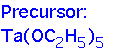
Almost all work on CVD of tantalum oxide has employed tantalum pentaethoxide as the precursor. It is stable in storage and not particularly toxic. However, it isn't very volatile. Temperatures over 100 °C are necessary to transport significant amounts of the vapor, necessitating the use of heated plumbing and chamber walls. Direct liquid injection for metering is commonly employed.
The oxide film is readily deposited at 400-450 °C in oxygen. Typical conditions are 0.4 to 2 Torr, with deposition rates of 5 nm/min. Film thickness used is around 10 nm, so high rates are unnecessary. Uniformity is almost wholly dependent on temperature control. Conformality is excellent.
The films are typically amorphous for low temperature deposition, but can be crystallized by extended anneals at > 700 °C. Most films have significant residual carbon, and oxygen vacancies, which cause high electrical leakage, especially after the heat treatment associated with e.g. flow of a BPSG layer after the capacitor dielectric. Various methods have been explored to reduce leakage:
- furnace anneal in oxygen at 800 °C
- ozone anneal at 450 °C combined with furnace oxygen anneals
- rapid thermal anneal (RTA) at 800 °C in N2O
- furnace anneal in N2O at 800 °C
- intentional crystallization of the film
- complete avoidance of temperatures > 500 °C after Ta2O5 deposition
Integration: Bottom Electrode
The performance of a DRAM capacitor dielectric is often characterized in terms of the equivalent oxide thickness: the amount of silicon dioxide which would give the same capacitance per unit area. The dielectric constant of "bulk" Ta2O5 suggests that a 100 Å film should give an equivalent oxide thickness of about 15 Å, but values of 25-35 Å were more typically observed. The problem turns out to be a result of the diffusion of oxygen to the silicon surface during the deposition process, forming a thin layer of silicon dioxide whose capacitance is in series with the Ta2O5 capacitance:
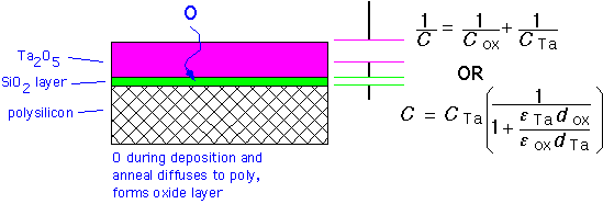
One solution is to expose the sample to ammonia for about 60 seconds in an RTA unit at 800-950 °C, causing a thin silicon nitride layer to grow on the surface. The nitride layer is resistant to oxidation and has a higher dielectric constant than oxide.
Integration: Top Electrode
If polysilicon is deposited directly onto the tantalum oxide layer, increased electrical leakage is observed after annealing. Titanium nitride (TiN) can be used as a top electrode without encountering the leakage problem, but the TiN oxidizes and cracks during any subsequent high-temperature anneal in an oxidizing ambient. An acceptable solution is to use a sandwich structure: tantalum oxide / titanium nitride / polysilicon.
The deposition method of the TiN is also of importance. Sputtered TiN fails to protect the edges of the post, leading to sporadic leakage problems. CVD TiN from TiCl4 and NH3 works very well if annealed after deposition in NH3 to reduce the chlorine concentration in the film.
- - - - - - - - - -
References:
"Trends in DRAM Dielectrics" K. Tang, W. Lau and G. Samudra Circuits & Devices May 1997 p. 27
"Ta2O5 capacitors dielectric material for Giga-bit DRAMs" Y. Ohji, Y. Matsui, T. Itoga, M. Hirayama, Y. Sugawara, K. Torii, H. Miki, M. Nakata, I. Asano, S. Iijima, and Y. Kawamoto, IEDM 95 p. 111
"1 G DRAM Cell with Diagonal Bit-Line (DBL) Configuration and Edge OPeration MOS (EOS) FET" K. Shibahara, H. Mori, S. Ohnishi, R. Oikawa, K. Nakajima, Y. Kojima, H. Yamashita, K. Itoh, S. Kamiyama, H. Watanabe, T. Hamade and K. Koyama, 1994 IEDM p. 639
"Low-Temperature Integrated Process Below 500°C for thin Ta2O5 Capacitor for Giga-Bit DRAMs" Y. Takaishi, M. Sakao, S. Kamiyama, H. Suzuki and H. Watanabe, IEDM 1994 p. 839
"Ta2O5 Capacitors for 1 Gbit DRAM and Beyond" K. Kwon, I. Park, D. Han, E. Kim, S. Ahn, and M. Lee, IEDM 1994 p. 835
"Highly Manufacturable Process Technology for Reliable 256 Mbit and 1 Gbit DRAMs" H. Kang, K. Kim, Y. Shin, I. Park, K. Ko, C. Kim, K. Oh, S. Kim, C. Hong, K. Kwon, J. Yoo, Y. Kim, C. Lee, W. Paick, D. Suh, C. Park, S. Lee, S. Ahn, C. Hwang and M. Lee, IEDM 1994 p. 635
"Highly Reliable, High C DRAM Storage Capacitors with CVD Ta2O5 Films on Rugged Polysilicon" G. Lo, D. Kwong, P. Fazan, V. Mathews, and N. Sandler, IEEE Electron Device Lett 14 216 (1993)
"A New Post-Deposition Annealing Method Using Furnace N2O for the Reduction of Leakage Current of CVD Ta2O5 Storage Capacitors", S.C. Sun and T.F. Chen, IEDM 1996 S27-4
"Electrical Characterization of CVD TiN Upper Electrode for Ta205 Capacitor", Myoung-Bum Lee, Hyeon-Deok Lee, Byung-Lyul Park, U-In Chung, Young-Bum Koh and Moon-Yong Lee, IEDM 1996 S27-3
Return to Tutorial Table of Contents
Book version of the CVD Tutorial